


Synopsys has introduced the industry’s first full-stack AI-powered suite of electronic design automation tools that covers all stages of chip design, from architecture to design and implementation to manufacturing. The Synopsys.ai suite promises to radically reduce development time, lower costs, improve yields, and enhance performance. The set of tools is set to be extremely useful for chips set to be made on leading-edge nodes, such as 5nm, 3nm, 2nm-class, and beyond.
Chip Design Challenges
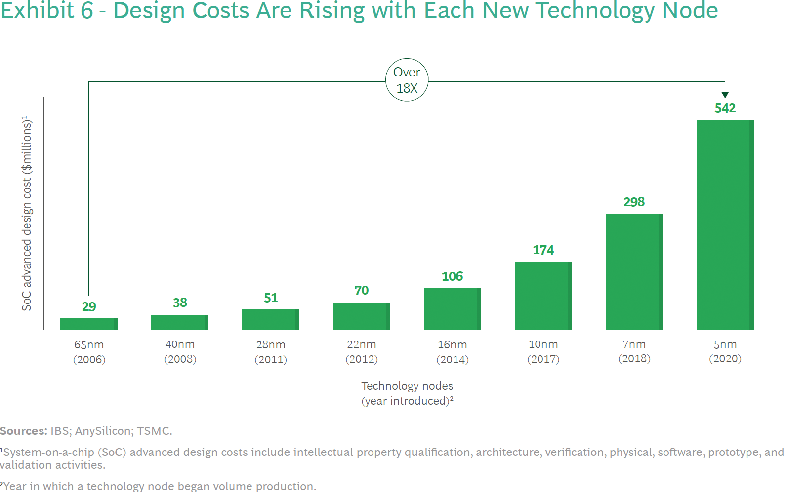
As chips gain complexity and adopt newer process technologies, their design and manufacturing costs escalate to unprecedented levels. Designing a reasonably complex 7 nm chip costs about $300 million (including ~ 40% for software). In contrast, the design cost of an advanced 5 nm processor exceeds $540 million (including software), according to International Business Strategies (IBS) estimates. At 3 nm, a complex GPU will cost about $1.5 billion to develop, including circa 40% for software.
The traditional ‘waterfall’ semiconductor design approach is perhaps one of the reasons why chip development costs skyrocket so rapidly. It takes hundreds (if not thousands) of engineers and thousands of servers over several years to develop and simulate architectural, structural, logic, and layout designs. Meanwhile, every design stage involves tasks that are essential for the quality of the chip, but they are iterative and time-consuming in nature. For obvious reasons, as chips get more complex, each design change gets longer as companies cannot throw in as many engineers as they want to a given task because the number of people they have is limited.
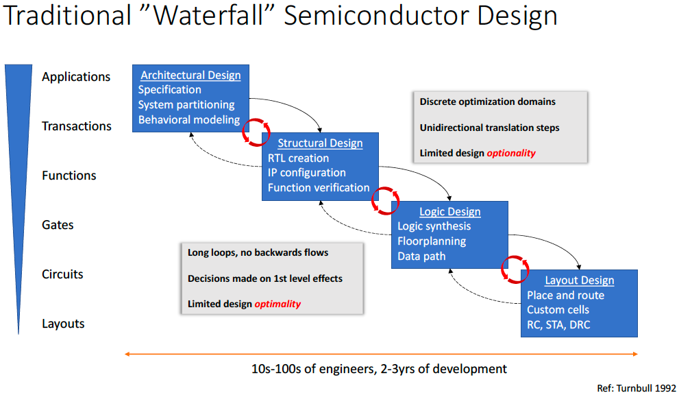
Things get more challenging as the waterfall approach almost excludes backward flows, so people implementing one of the thousands of possible place and route designs have little to zero influence on the architectural or structural design. As a result, the only way to avoid inefficiencies resulting in higher-than-expected costs, lower-than-expected performance, and/or higher-than-expected power consumption is to make different design teams work closer together at all stages. Yet, this gets harder as design cycles get longer.
Manufacturing costs at 5 nm and 3 nm production nodes are also noticeably higher than those on previous-generation fabrication technologies. The latest leading-edge manufacturing processes extensively use extreme ultraviolet lithography and more expensive raw materials (e.g., pellicles for photomasks, resists, etc.). Therefore, it gets even more crucial for chip developers to build close-to-perfect designs that are cheaper to make.
In general, the semiconductor industry faces several challenges these days as it needs to cut down development time, maintain (or even reduce) chip development costs, and ensure predictable manufacturing costs. Everything has to be done when the industry faces a deficit of highly skilled engineers.
This is where the Synopsys.ai EDA suite comes into play.
From Scratch to High-Volume Manufacturing
The Synopsys.ai full-stack EDA suite consists of three key applications the DSO.ai AI for chip design: the Synopsys VSO.ai for functional verification, and the TSO.ai for silicon test. The suite is designed to speed up iterative and time-consuming chip design stages using machine learning and reinforcement learning accelerated by modern CPUs and GPUs.
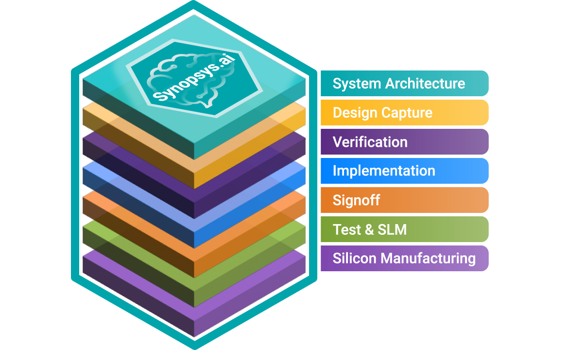
Synopsys has been offering its DSO.ai place and route AI-driven solution for about two years now, and over 100 designs have been taped out using the EDA tool so far. But this time around, the company is looking at fast-tracking all design stages with AI. The software suite can be used at all stages, including simulations, design capture, IP verification, physical implementation, signoff, test, and manufacturing.
Better Architectures Delivered Faster
Small groups of very talented engineers typically develop microarchitectures, and this stage is considered by many as an intersection of technology and art. In fact, microarchitectures are developed fairly quickly too. Synopsys says that even this stage can be accelerated and improved with AI as artificial as, unlike people, machines can quickly estimate the most efficient architecture parameters and data paths.
The General Manager of Synopsys’s Electronic Design Automation Group (EDA), Shankar Krishnamoorthy, states, “The whole process of developing a chip starts with the architecture of the chip and there are a lot of decisions to be made there,” He also went on to say “How big does your cache need to be? What kind of interfaces run between your computer and memory? What