


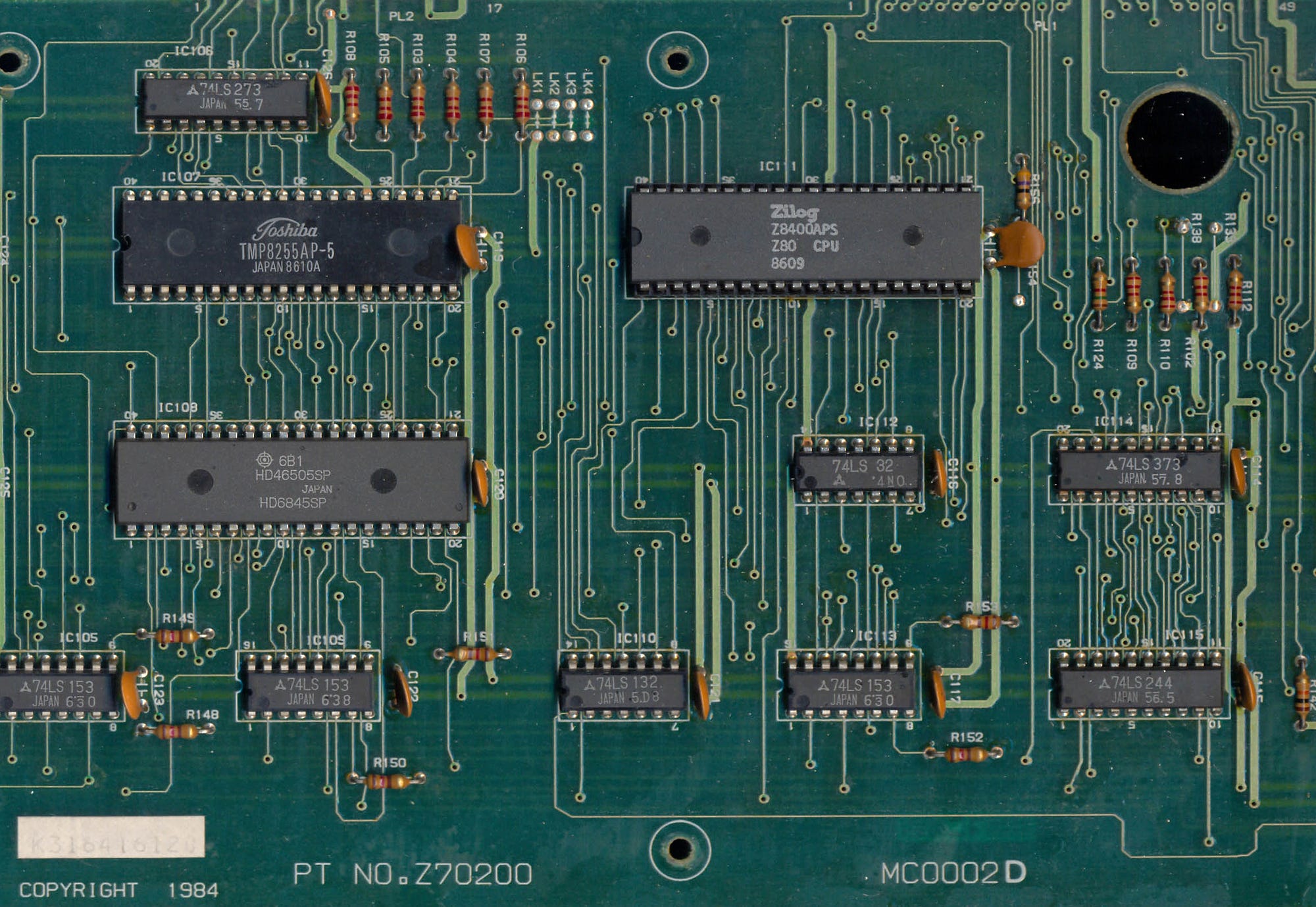
In the early 1980s, a typical printed circuit board inside an 8-bit home computer looked roughly like this:
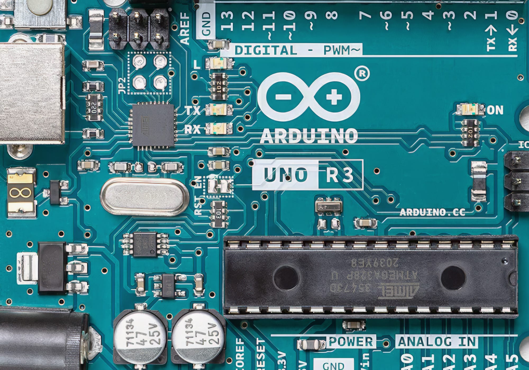
By the early 2010s, the same tech would be packaged the following way:
Other than increased miniaturization, the most striking change is the use of copper pours — that is, computer-generated zones that occupy the empty space between individual traces on a PCB.
Why did we start doing this? One hand-wavy answer is that in high-speed electronics, the practice can improve signal integrity. This made the approach essential in some cutting-edge applications, such as smartphones or desktop computers. But of course, we’re not looking at that.
Another change is that in the 1980s, the FCC started applying its 47 CFR Part 15 rules on “unintentional radiators” to a wide range of computing devices. It’s a bit of a racket: you need to submit prototypes to an accredited laboratory, pay big bucks for RF testing, and face additional costs and delays if you don’t pass. Copper pours can reduce RF emissions, so they’re often incorporated just in case.
Last but not least, the change is a matter of fashion: hobbyists egg each other on to copy industry trends. Unusual or outmoded PCB aesthetics are often frowned upon, even if the critics can’t quite explain what’s wrong with the design.
But hold on, let’s address the elephant in the room: why do copper pours do anything in the first place?
The following discussion assumes familiarity with such as inductance or reactance. If you need a refresher, start with this article first.
In electronic circuits, the flow of electrons is confined to conductors, but the transfer of energy doesn’t involve these particles bouncing off each other; instead, the process is mediated through electromagnetic fields. These fields originate from charge carriers, but extend freely into the surrounding space.
Certain materials, such as ferrite, respond to external magnetic fields by rearranging their own valence electrons; this extracts energy from the surrounding field. If the field originated from a nearby conductor, the flow of current in that conductor is momentarily hindered. The ferrite eventually reaches saturation, but any subsequent changes in conductor current will be once again impeded until a new equilibrium is reached.
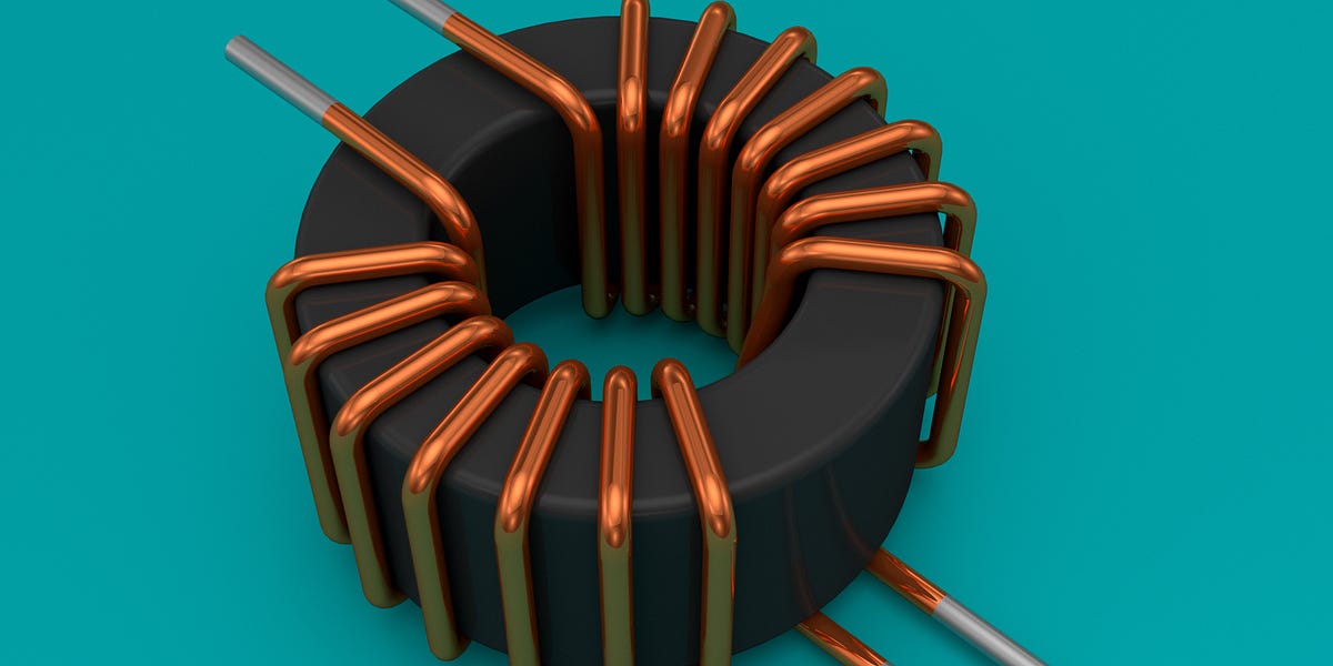
This is the behavior of a standard inductor, but a clever variation of the theme is the common-mode choke. Its most basic form is an accessory seen on some computer cables: a tubular ferrite element with two wires passing through in the same direction. A more compact version uses a smaller toroid, each conductor wrapped around to make the signal pass front-to-back a couple of times:
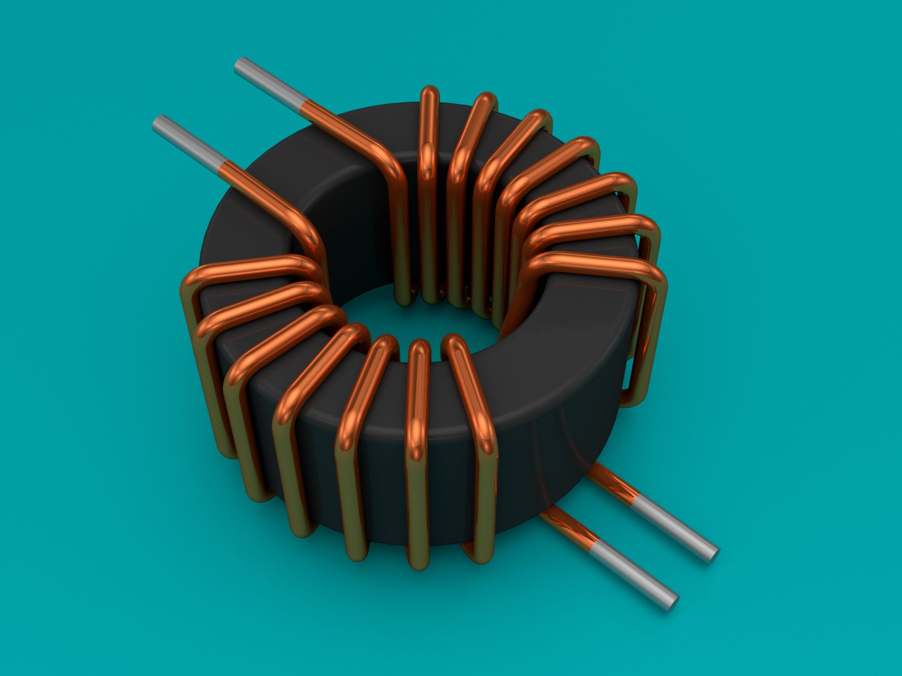
If there is a common-mode current flowing through both wires in the same direction, the result is a coherent magnetic field acting on the ferrite. This makes the device behave like a run-of-the-mill inductor, passing through DC but attenuating higher-frequency components.
Conversely, if there are complementary currents flowing in opposite directions — as would be the case for a differential signal pair or the “+” and “-” wires connecting to a power supply — the resulting fields net out to zero. This precludes magnetization; with no energy soaked up by the ferrite, the device’s inductive reactance (a resistance-like measure of how much it attenuates AC signals) stays low.
One possible use of such chokes is the suppression of RF pickup on long cables. Radio interference typically produces the same electromotive force in all bundled conductors, so the resulting currents are common-mode and can be separated from the differential signals we care about.
Right. The phenomenon of inductance is not limited to ferrite cores; it is present, albeit to a much smaller extent, for any trace on a PCB.
To understand why this matters, let’s consider the following board. It has a si