


Introduction
When we develop FPGA based solutions of course we make use of all the IP which we possibly can, as this accelerates the development. However, there are always cases where we need to generate custom IP cores using our hardware description language of choice.
Developing and verifying this IP blocks brings with it several challenges, which can make a project be a little more painful if it is not done correctly.
Of course one of the key things we need to think about when working with the FPGA is we need to first think about the the functionality we wish to implement, along with a following the correct development process.
For this example we will be using the following process
- Define Requirements
- Create Micro Architecture and Interfacing
- Write the RTL description of the module
- Develop a Bus Functional Model of the interfaces for the RTL
- Create a test bench for the verification
Requirements
For this project we are going to create a simple QSPI Slave interface to AXI Stream this will have the following requirements.
These requirements are pretty simple to create the module. We could then integrate the module with a previous project to access the AXI4 network within a chip over QSPI.
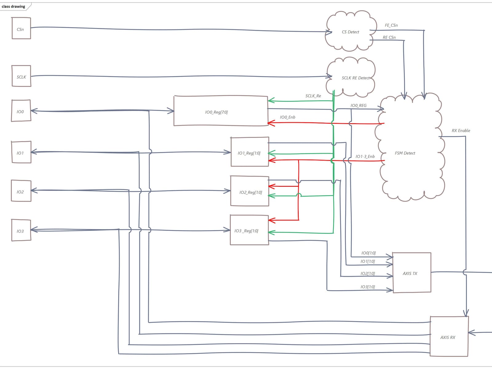
Micro Architecture and Interfacing
From this we need to create the micro architecture which means we need to understand how QSPI in serial memory mode works.
The waveforms for the READ4IO and PP4IO can be seen below
What is interesting about the waveforms is they first use a single line to IO0 to send in the command either 0x38 for write or 0xEB for a read operation.
Once the command has been sent the remainder of the transaction is performed using all IO lines.
The impacts on our architecture are that we need a 8 element shift register for the IO0 and two element shift registers for IO1-3. Once the command has been received we are able to use just the lower two elements of the IO0 registers.
Our micro architecture therefore needs to be able to do the following
- Detect a new transaction by identifying falling edge on CSn
- Detect a rising edge on the SCK once a new transaction is enabled
- Enable data to be shifted into IO0 register
- Once 8 bits of data are in IO0 register depending check for valid read or write command
- For Write enable IO1-3 along with IO0 – Every two SCLK output a byte of data on the AXIS Interface. Ensure IO drivers are Tristate in that state.
- For Read, during the dummy clock cycles, read from the AXIS interface
- For Read at the end of the dummy cycles output the data on IO0-IO3
- De assertion of CSn stops the transaction and